|
|
|
 www.design-reuse-china.com
 |
|
 |
| D&R中国官方微信公众号, 关注获取最新IP SOC业界资讯 |

Security that Builds Value: Managed NAND as a Foundation for IoT Security

intrinsic-id.com, Sept. 14, 2021 –
在 NAND 控制器内使用 SRAM PUF生成并安全存储加密密钥为存储器供应商及其客户提供了诸多好处:
- 安全性:
- SRAM PUF 生成所有安全场景在之建立的基本设备根密钥,并从该密钥中派生额外所需密钥
- 所有根密钥和派生密钥不在任何内存中实体存储,使攻击者无法看到它们
- 所有密钥均基于设备的物理特性,无法复制,抵御内存被克隆与伪造
- 灵活性:
- 所有密钥均于设备内部创建,无需外部配置,排除在受信任设施中进行安全配置
- 因可在软件中内置,SRAM PUF 支持诸如无线更新和棕地部署等面向未来的解决方案
- 低成本:
- 为物联网设备创建安全且无需额外硬件措施:
- 无需OEM创建安全区域实现存储密钥
- 内存供应商无需再对模块中的密钥进行任何物理保护
One of the fastest growing markets in the semiconductor industry is that of non-volatile memory (NVM). Among the main drivers for this enormous growth in data generation are vast movements towards cloud storage, the Internet of Things (IoT), and autonomous driving.
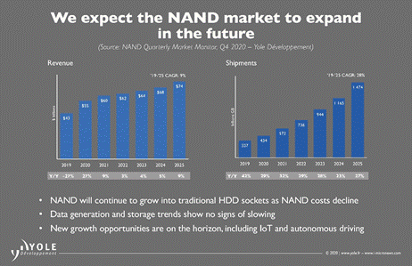
Figure 1.NAND flash market growth, as projected by Yole Développement (Q4, 2020)
This trend comes with requirements for a lot of memory for datacenters and mobile devices. Simultaneously, traditional forms of storage, such as optical tapes and old hard drives, are being replaced by newer technologies, such as solid-state drives and all-flash devices. All these markets expect double-digit growth in the next years.
As the IoT continues to expand rapidly, NVM is also becoming increasingly important for IoT devices themselves. This becomes clear from the "Other" category in Figure 2 that shows IoT devices for vertical markets such as medical, industrial and consumer, which has an expected CAGR of 33%.
Figure 2. NAND flash in different vertical markets, as projected by Yole Développement (Q4, 2020)
On IoT devices, NVM holds the valuable data, software, and firmware that need to be stored permanently. Most microcontroller units (MCUs) for IoT have very little or no discrete NVM for storing this data, which is why an additional NVM chip is implemented inside of an IoT device, next to the MCU, the sensors and the connectivity chips.
Managed NAND Flash: A New Risk for IoT Devices?
Along with new opportunities come new needs; for IoT devices – and their components – that new need is increased security. Well-publicized attacks on IoT devices, such as pacemakers, baby monitors, and thermostats, demonstrate why manufacturers need to be security conscious.
OEMs will typically equip their products with MCUs that contain a broad range of security capabilities, such as hardware cryptographic accelerators, random number generators and secure embedded memory. However, it is typically the storage media – in this case, a managed NAND flash – that holds most of the OEM's precious intellectual property (IP). Unfortunately, such storage media have traditionally been more vulnerable than the MCUs. This is because the managed NAND flash is a separate module, with its own interface on the board that can be accessed quite easily by skilled attackers. The availability of a direct interface to the memory (which is not the case with discrete NVM inside the MCU) leads to the possibility for attackers to read or change sensitive data inside the memory. And without proper authentication, the NAND flash can be switched out for a malicious/counterfeit one. Such attacks not only put the IP stored in the device at risk, but also the entire network the device is connected to.
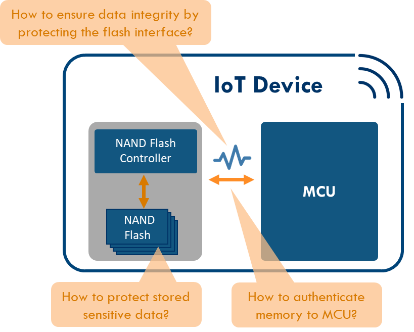
Figure 3. Typical security challenges for managed NAND flash
But what if you could overcome NAND's weakness by adding strong security primitives that transform it into the foundation for system-level security, providing the opportunity to create more value to all stakeholders involved?
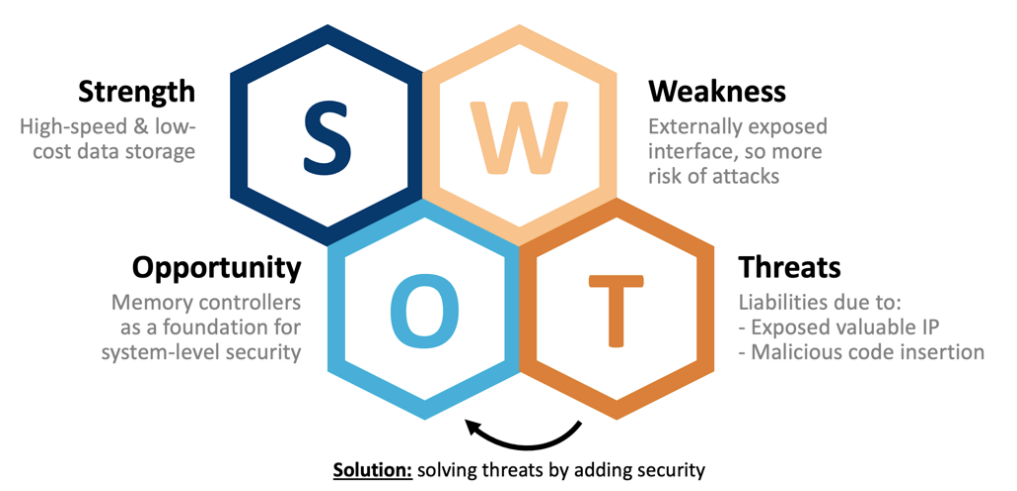
Figure 4. SWOT analysis for external NVM in IoT
Making Managed NAND the Security Guard Using PUFs
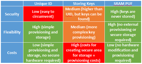
There are several established methods for implementing security in flash controllers. A traditional method is deploying a unique ID (UID), which uses a pairing protocol with the MCU to establish secure communications. Without the correct UID, the MCU will not read data from the flash. However, UIDs have been shown to be easily exposed, even by non-expert attackers. This allows attackers to circumvent the pairing, swap out managed NANDs between devices, and make unauthorized copies of the flash content. So, without the ability to keep the UID secret, there is no root of trust, and no security.
The use of secret cryptographic keys offers better security than a UID. However, the managed NAND flash must be equipped with such a cryptographic key and the key must be kept secure. Keys cannot be stored next to the data they are supposed to be protecting, because attackers will easily be able to read, copy, or alter these keys through the interface of the module. So, storage in the NAND flash is not an option. Any key that is physically present in the memory – even if it is shielded – is vulnerable to physical attacks. This means the keys should remain inside the NAND flash controller at all times. However, most controllers do not provide a secure area appropriate for key storage, and even those that do offer varying levels of security. In addition, the keys must be provisioned into these controllers, which is non-trivial. And again, storing keys in unprotected memory, even inside the controller, means risking hardware attacks.
The alternative approach that alleviates the burden of externally generating and securely storing root keys in a NAND flash controller is to employ an SRAM-based Physical Unclonable Function (PUF). SRAM PUFs use the behavior of conventional SRAM memory that is typically available in the controller to extract a unique pattern or "silicon fingerprint." This fingerprint is virtually impossible to clone or predict, and because it is inherent to the silicon, keys based on this fingerprint aren't externally provisioned, but intrinsically generated from the chip itself.
How does it work? An SRAM memory consists of a number of SRAM cells. Each SRAM cell consists of two cross-coupled inverters that each are built up by a p- and n-MOS transistor. When power is applied to an SRAM cell, its logical state is determined by the relation between the threshold voltages of the p-MOS transistors in the invertors. The transistor that starts conducting first determines the outcome, a logical '0' or '1.' Every time the SRAM is powered, every SRAM cell has its own preferred state resulting from the random differences in the threshold voltages. This preference is independent from the preference of the neighboring cells and independent of the location of the cell on the chip or on the wafer. Hence, every SRAM region yields a unique and random pattern of 0s and 1s, which is called the "silicon fingerprint" or SRAM PUF.
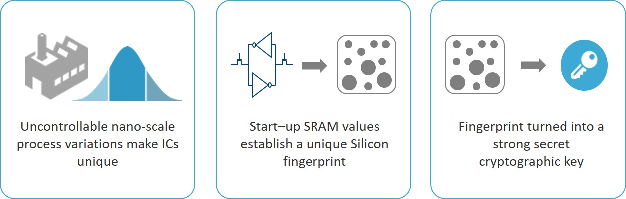
Figure 5. SRAM PUFs: turning nano-scale process variations into unique cryptographic keys
hese silicon fingerprints can be turned into master keys that establish a reliable root of trust. Whenever the root key is needed by the system, it is reconstructed without the need for storing this root key in any form of memory. This means that when the device is powered off, no secret key can be found; in effect, the root key is invisible to attackers. A whole tree of cryptographic keys can be created from this root PUF key, providing a flexible mechanism for key provisioning.
To make SRAM PUF technology available for protecting managed NAND flash, solutions are now available in software that can be installed on the processor of the NAND flash controller, making them easy to add to existing hardware. Typical NAND flash controller processors have access to SRAM, either internally or in the buffer of the controller. This SRAM can be used to create the SRAM PUF fingerprint, enabling the managed NAND to create cryptographic keys simply from its own unique silicon structure.
The cryptographic keys remain inside the processor, never leaving the boundaries of the controller, and become the basis of security. Having these strong cryptographic keys inside the NAND flash controller protects the flash content and its interfaces, while being able to authenticate the managed NAND to the MCU and even adding the unclonable device identity that is the foundation for cloud services to securely authenticate the IoT device and setup secure communications. Hence, a standard managed NAND flash is turned into the valuable foundation for system-level security of an IoT device.
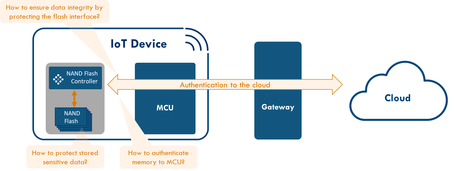
Figure 6. Resolving security issues and adding value by using SRAM PUF in NAND flash controller
Using SRAM PUFs to generate and securely store cryptographic keys inside of NAND controllers provides many benefits for memory vendors and their customers:
- Security:
- SRAM PUFs create the fundamental device root key upon which all security scenarios are built and from which all additionally required keys are derived
- All root keys and derived keys are never physically stored in any memory, making them invisible for attackers
- All keys are based on the device's physics, so they cannot be copied, which makes the memory immune to cloning and counterfeiting
- Flexibility:
- All keys are created from within the device itself and never have to be provisioned externally, eliminating the need for secure provisioning in a trusted facility
- Because of the possibility to implement in software, SRAM PUFs allow for future-proof solutions that include over-the-air updating and brownfield deployment
- Low Costs:
- No additional hardware measures are required to create secure IoT devices:
- No need for OEMs to create secure area for storing secret keys
- Memory vendors no longer require any physical protection for keys in module
- No additional hardware measures are required to create secure IoT devices:
About the author: Vincent van der Leest is the Director Product Marketing for Intrinsic ID in Eindhoven, The Netherlands. Intrinsic ID provides its SRAM PUF technology to many of the world's largest semiconductor companies, including companies like NXP, Silicon Labs, and Intel. Intrinsic ID IP has also been vetted for use in Government & Defense projects.
To learn more about how you can turn your NAND flash controller into a security guard for software and data integrity, device authentication and anti-counterfeiting for IoT devices, please visit www.intrinsic-id.com.