|
|
|
 www.design-reuse-china.com
 |

|
 |
| D&R中国官方微信公众号, 关注获取最新IP SOC业界资讯 |

Ams Breaks Ground on N.Y. Fab

By Jessica Lipsky, EE times,SAN FRANCISCO, Apr. 20, 2016 – Ams AG broke ground on a wafer fab in upstate New York today (April 20), joining the ranks of advanced manufacturers in the region. The Austrian company aims to start volume ramp of high-performance analog wafers by the second half of 2018.
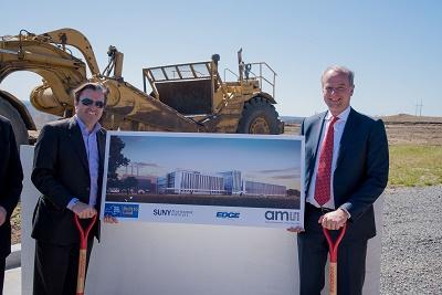
Source: AMS
Production capacity at the Utica fab will supplement ams' existing 180nm and 350nm CMOS and SiGe fab at its headquarters near Graz, Austria. The fab will initially offer capacity of at least 150,000 200mm wafer equivalents per year, then expand to a capacity of more than 450,000 200mm wafer equivalents per year.
Ams' Unterpremstaetten fab is mature and running at close to capacity so it was known that ams was in the market for a new manufacturing site. The new facility will sit on a 450-acre site on vacant land belonging to State University of New York SUNY at Marcy between Utica and Rome, northwest of the state capital of Albany. Adding this additional volume to its in-house chip manufacturing facilities will allow the company to meet increasing demand for sensor solution ICs, ams said in a release.
"By operating our own in-house wafer manufacturing facilities, ams is able to push the limits of sensor manufacturing, assuring customers a dedicated supply of sensors with the highest quality standards," ams' CEO Alexander Everke told EE Times.
The financial burden of building a fab does not solely fall on ams-the fab will be built by the State of New York and then rented by ams under a 20-year lease. The public-private partnership is part of Governor Andrew Cuomo's Nano Utica initiative, which aims to bring 4,000 jobs to the region over the next decade. The initiative is designed to replicate SUNY Poly's nanotech megaplex in Albany, which houses the College of Nanoscience and Engineering and many collaborative research efforts among large semi industry giants.
This non-traditional ownership arrangement will provide ams with no depreciation and significant cost-per-wafer benefits, EE Times earlier reported. Ams has no plans to lease out production space to other companies a la Samsung.
Click here to read more...