|
|
|
 www.design-reuse-china.com
 |

|
 |
| D&R中国官方微信公众号, 关注获取最新IP SOC业界资讯 |

Chipus Microelectronics becomes an official Silterra's design partner
Oct. 25, 2016, Oct. 25, 2016 –
Working in cooperation for the last 5 years and serving several Silterra customers with key Analog and Mixed-Signal Ultra-Low-Power IPs, Chipus was recognized for its effort and success by Silterra as an official Design Partner.
'Chipus is excited to continue serving Silterra customers and committed to keep improving its list of ultra-low-power IPs, accelerating the plethora of battery-powered IoT devices that will explode in the market in the next years', says Chipus CEO Murilo Pessatti.
The Malaysian foundry started its operations in 2000, with maximum production capacity of 40.000 wafers/month.
'Chipus has been accumulating a significant amount of expertise in Silterra CMOS and BCD technologies, by providing great support to key SilTerra Customers in ultra-low-power analog and mixed-signal IPs for the last 5 years', says Pankaj Gadani, Senior Sales Director of Silterra.
Chipus has 180+ IPs in its portfolio.
Highlights:
- CM1711ff - Li-Ion Battery Charger
1% Accuracy (4.2V), up to 1500mA fast charge, reverse current protection, integrated power FET and sensing, charge from AC and USB, built-in NTC. - CM9011ff - UHF Passive RFID Analog/RF Front End
Compliant with EPCGlobal Class 1 Gen 2 / ISO18000-6C. Complete analog/RF front end, with rectifier, demodulator, backscattering modulator, power management unit, persistence flag generator, featuring 1.5microA current consumption.
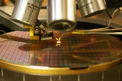
Pilot lot wafer with CM9011ff IP.
About Chipus
Chipus Microelectronics is a semiconductor company specialized in the development of low-power, low-voltage, analog and mixed-signal intellectual property (IP) blocks for integrated circuits (ICs) and systems on chip (SoCs). It develops configurable IP core architectures that allow a good level of customization together with high IP portability, providing unique level of freedom on customer design requirements. Chipus is headquartered in Florianopolis - Brazil, with a Sales office in Santa Clara - California and a Sales Representative in Europe.
For additional information on Chipus or its services, please visit: www.chipus-ip.com
About Silterra
SilTerra Malaysia Sdn Bhd is a semiconductor wafer foundry offering major fabrication and design support services in CMOS logic, High-Voltage, Mixed-signal, RF and MEMS technologies down to 90 nanometer feature size. SilTerra's wafer fab has a design-in capacity of 40,000 eight-inch wafers per month and currently serves customers in US, Taiwan, Korea and China.
Environmentally vigilant, SilTerra delivers award winning, world-class performance to its customers seeking flexible capacity, custom technologies, competitive advantages and around the clock customer support. SilTerra is ISO 9001:2008 and ISO 14001 certified. Starting commercial production in 2001, the company's headquarters and factory are located in Malaysia's Kulim High-Tech Park, with sales and marketing offices in San Jose(California) and Hsinchu(Taiwan).
For additional information on SilTerra or its services, please visit: www.silterra.com