|
|
|
 www.design-reuse-china.com
 |

|
 |
| D&R中国官方微信公众号, 关注获取最新IP SOC业界资讯 |

Attopsemi's I-fuse OTP Passed 3 lots of HTS and HTOL Qualification for 1,000hr on GLOBALFOUNDRIES 22FDX FD-SOI Technology


Attopsemi's I-fuse™ provides small size, high reliability, low program voltage/current, low power and wide temperature to enable GLOBALFOUNDRIES 22nm FDX® for AI, IoT, automotive, industry, and communication applications
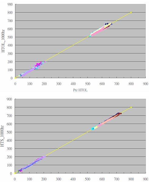
Santa Clara, California, Mar. 12, 2019 – Attopsemi, an OTP IP provider, announced today that the company's 256Kb OTP (One-Time Programmable) IP passed 3 lots of 150°C HTS and and 125°C HTOL for 1,000 hours following the JEDEC standards. Not only all 120Mb in 3 lots of HTS/HTOL passed functionally, the cell currents did not show any variations after stresses. The defect rate is less than 0.01ppm. This is a phenomenon as most other OTPs show severely parameters shifted and tailing bits after HTS/HTOL stresses. The X/Y plots of cell current in post-stress versus pre-stress are shown in the followings:
"Other than high reliability, I-fuse™ can be programmed at 1.0V with only 1.0mA of program current, said Shine Chung, Chairman of Attopsemi, "Because of no need for charge pumps, our I-fuse™ OTP size can be only 1/4 to 1/5 of the competing OTP technologies." "Moreover, I-fuse™ can work at wide temperature range of from -55oC to 150oC without needing any redundancies, ECC, or twin cells." Our I-fuse™ also offers high data security and full testability unseen in any other OTPs." This IP also passed 250oC HTS wafer-level burn-in in a previous press release:
"We sincerely appreciate all the supports from GF in developing our proprietary I-fuse™ OTP technology on 22FDX®," said Shine Chung, Chairman of Attopsemi. "After many years of dedicated works and collaboration with foundries and customers worldwide, our I-fuse™ technology has finally been demonstrated as OTP of choice. We have proven that I-fuse™ can ensure high reliability with smaller size by using a fraction of program current. With our superior OTP IP, we expect to bring substantial benefits to all semiconductor communities."
About Attopsemi Technology
Founded in 2010, Attopsemi Technology is dedicated to developing and licensing fuse-based One-Time Programmable (OTP) IP to all CMOS process technologies from 0.7um to 7nm and beyond with various silicided polysilicon and HKMG technologies. Attopsemi provides the best possible OTP solutions for all merits in small size, high quality, high reliability, low power, high speed, wide temperature and high data security. Attopsemi's proprietary I-fuse™ OTP technologies have been proven in numerous CMOS technologies and in several silicon foundries.